
A little history
Among the variety of components that make up HPF, the mammoth 10m Hobby-Eberly Telescope and the hefty 200lb diffraction grating are certainly the most imposing. Although these are among the best and most advanced tools in modern astronomy, they would be fundamentally recognizable to astronomers from before the modern era: Galileo Galilei was an enthusiastic promoter and salesman of telescopes during the early 17th century and Joseph von Fraunhofer first used a prism to refract and study the spectrum of sunlight in the early 19th century.

An early Dutch telescope – “Emblemata of zinne-werck” (Middelburg, 1624)
These early astronomers would certainly be impressed by the tiny 2 square-inch piece of semiconductor sitting at the heart of HPF. This tiny device is what will record the infrared (IR) light from M dwarf stars that HPF will study, changing the photons from the star into electrons that can be processed by electronics and computers. In a sense this detector is the fundamental piece of technology that makes HPF possible.
Up until the late 19th century, the only detector astronomers had at their disposal was the human eye. Fortunately, the human eye contains an excellent light detector: our photosensitive rod and cone cells (along with the constant adjustment of the iris) allow us to see a wide spectrum of light with an impressive dynamic range. So these early astronomers were able to explore the solar system and solar neighborhood, and even to study the spectra of bright objects.

Fraunhofer demonstrates his spectroscope – Richard Wimmer – “Essays in astronomy” – D. Appleton & company, 1900
Two significant issues with “eyeball” observations are: 1) The eye doesn’t have a “long-exposure” mode, familiar from digital cameras (HPF team member Stefansson is an expert), in which images and details can be made out in very dark scenes, simply by exposing for a long time. 2) The eye cannot see large portions of the electromagnetic spectrum, including regions like the infrared, where M dwarf stars emit most of their light.
Moving beyond the eye
The need for sensitivity to low light levels was addressed by the development of photographic emulsion plates in the late 19th century. Astronomers could place these plates at the prime focus of a telescope, and expose them for several minutes or longer, revealing details invisible to the naked eye. Despite the inefficiency of these plates (only ~1% of the incoming light was actually recorded), they enabled numerous foundational discoveries, including the structure of stellar populations, the calibration of various techniques for measuring distance (a perennial issue in astronomy), and the expansion and scale of the universe. By the middle of the century, though, the use of these plates has started to reach its limit.

Hubble at the prime focus of the Palomar telescope, where the photographic plates would be placed. He used these plates to discover the existence of other galaxies (island universes) besides our own, and the expansion of the Universe. – AIP: Ideas of Cosmology
The 1960’s saw the key development that ushered in the modern era of astronomy: the invention of systems that could directly turn light into electrical charge. Charge-coupled devices (CCDs), as they are known, not only put astronomical images and spectra directly into a form that computers can understand, but they are vastly more efficient than photosensitive materials (up to 80-90% of the incident light can be recorded). Instead of going to an observatory and obtaining photographic plates, astronomers could put their data onto tapes or discs, or (much later on) simply transfer them over the internet.
What exactly is a CCD?
CCDs are generally made of silicon (Si) semiconductor, a material that is somewhere between an electrical insulator and conductor. It has electrons in its structure that can be excited into the “conduction band,” which allows them to move around (ie carry current). CCDs are structured so that light (photons) excite these electrons, allowing a count of how much light (how many photons) have been observed. By printing millions of these tiny photo-sensitive elements (pixels) in a grid, and putting it behind the lenses of a camera, one can record images with remarkable fidelity, entirely electronically.
In a CCD, the semiconductor material is doped with certain materials and layered to create an array of tiny pixels, in which the electrical fields can be precisely manipulated. The result is that a given pixel can spend some time exposing (turning photons into electrons), and then can send its accumulated charge across the array (like a bucket brigade) to be read into a computer by an analog-to-digital convertor. The analog-to-digital converter measures the (continuous) voltage from the photo-excited electrons, and translates it into a discrete number that a computer can work with.
Energy levels for a metal, different types of semiconductors, and an insulator. The darkness corresponds to the density of electrons at the level, and the horizontal axis roughly indicates the density of states in a given material. The energy gap between valence (lower) and conudction (higher) bands for a semiconductor is small.
The rise and advances of Si-based CCDs was enabled by the rise of the hundred-billion dollar semiconductor industry, which provides the (incredibly pure) Si-based structures that underlie modern electronic devices. However, a limitation on Si-based CCDs is that the electrons need a kinetic energy of at least 1.1 eV (known as the “band gap”) to make the jump into the conduction band. This translates roughly to light with a wavelength of 1 micron; if the light has a longer wavelength (less energy) than this, it cannot excite the Si semiconductor electrons and will be invisible to the CCD. We are interested in looking at light from M dwarfs out to 1.3 microns with HPF, so we have to use a fundamentally different type of detector.
How about the infrared?
In the past few decades, new types of IR-sensitive detectors have been developed. These are based on the same principles as Si-based CCDs (detect charge with a semiconductor and process the resulting charge), but they use different types of semiconductors, which have smaller band gaps and are therefore able to detect IR light. These new detectors also have a different architecture for processing the charge and communicating with the controlling electronics: instead of sending the charge across the array it is read out directly at each pixel. They are called CMOS (complimentary metal oxide semiconductor) detectors, because they use CMOS design to fit the necessary components into each pixel.
The HPF detector
The detector we will use for HPF is made up of 2048 x 2048 pixels, each 18 microns on a side. Each pixel (and the detector as a whole) is made up of two layers: the top semiconductor layer is made from a mixture of Hg, Cd, and Te (call it Mer-Cad-Tel), and the connected bottom layer is Si-based and handles the processing of the charge created in the top layer.
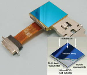
A hybrid CMOS detector much like the one that will be used in HPF. – OSA-OPN.org
The two layers are substantially different, and each is very interesting in its own right. The top layer of HgCdTe has to be just the right mixture of these elements in order to have the appropriate band gap for the ~1 micron light we want to observe. Importantly, we also want the detector to be insensitive to light that is redder (longer wavelength/lower energy) than this, because in this region of the spectrum thermal background radiation is a huge problem. The sky, the telescope, and the instrument itself can emit light at these wavelengths (>1.7 microns), and would easily overpower the starlight we want to observe. Fortunately, our detector has just the right mixture of Hg,Cd,Te to prevent it from being sensitive to the thermal background coming from the instrument’s surroundings (redder than 1.7 microns).

Spectrum of light coming from an M dwarf star, compared to that of the room temperature surroundings of the instrument.
The lower layer (the read out integrated circuit, or ROIC) is Si-based, and contains all the machinery necessary to amplify (source-follower), convert, and multiplex the signals of, and to control (reset, apply bias voltages), each pixel. This is quite impressive, since each pixel is only 18 microns on a side! The fact that each pixel has its own controls and readout mechanisms means that the detector is very flexible in how it can be operated. For example, we can address each pixel individually, reading them out or changing their bias voltages. This is very useful for running tests of the detector behavior, and can also be used for fun! (See the figure below, where we changed the biases on a small part of our engineering array to make letters).

Graffito on the engineering-grade array.
After each of these layers is independently fabricated, they are pushed together and “bump-bonded” to create the final detector array that we use.
Our detector was designed and manufactured by Teledyne Imaging Sensors, and the technology used was mostly developed in the build up to the James Webb Space Telescope, which will use a number of detectors of a similar type as ours. It is called a HAWAII 2-RG (or H2RG, or HgCdTe Astronomy Wide Area Infrared Imager, 2k x 2k pixels with Reference pixels and Guide mode, whew!) These detectors are of excellent quality: they have >70% quantum efficiency, very low noise characteristics (astronomers often worry about the “dark current” and “read noise,” which can mask small signals that you might be looking for). We actually have two of the same kind of detector: one “engineering” grade with a few cosmetic defects, which is not perfect, and one “science” grade, which is nearly perfect. The engineering grade detector is the one we use to develop the routines and characterization we need to make sure that we know how to use the science grade detector and how it will behave.
Despite the excellent characteristics of the detector, there are still some issues that we are working through:
- Persistence: Some of the pixels on these detectors will “remember” what happened to them, i.e. they still appear to have signal after they have been reset.
- Inter-pixel capacitance: Pixels can induce (fake) signals on neighboring pixels, since they can be capacitively coupled.
- Flux-dependent nonlinearities: Pixels can behave differently depending on the intensity of the light they are recording.
Each of these is a tiny behavior, but everything will matter for HPF, because the spectral Doppler (radial velocity) shift we are trying to measure corresponds to about 1/1000th of a detector pixel! We are currently working to understand these behaviors better on our engineering grade detector so that we will understand how our science grade array works when the time comes.
So…
The HPF detector will be the end of the road for the photons coming from M dwarfs we will study: after being born in the M dwarf photosphere, traversing light-years of interstellar space, bouncing off the HET mirror, winding down the optical fibers into the basement, and diffracting off the HPF gratings, the camera will focus them down onto the pixels, where their last action will be to kick an electron in the HgCdTe material. If the M dwarf is wobbling due to an orbiting planet, the Doppler shift will cause the successive photons to land in slightly different spots on the detector. Thanks to the impressive array of technology going in to HPF, especially the detector, we will be able to measure these shifts and discover new worlds.
 RSS - Posts